From photos
to KiCad drafts.
Turn PCB photos into component, pad, and visible trace candidates. Inspect the evidence, make corrections, and prepare a KiCad draft on your own computer.
Synthetic example board. Select a view above to explore its layers.
01 / THE WORKFLOW
Four steps to
understand the board.
A photo is the starting point. RA PCB brings visible evidence together in an editable workspace.
Photography and workflow guide- 01
Photograph both sides.
Use a fixed camera and sharp front and back images. Mark the board corners and shared alignment points.
INPUT / PNG · JPEG · TIFF - 02
Extract visible evidence.
Inspect component candidates, pads, copper traces, and readable markings on the same image.
ANALYSIS / LOCAL ONNX + OCR - 03
Resolve the uncertainties.
Correct inaccurate candidates. Compare pin mappings and connections with the physical board before confirming them.
EDITING / UNDO · REDO - 04
Move into a KiCad draft.
Calibrate the scale using a known distance. Export a schematic, physical PCB draft, netlist, and BOM.
OUTPUT / .KICAD_SCH · .KICAD_PCB
02 / THE DESKTOP WORKSPACE
Keep the image
behind every candidate.
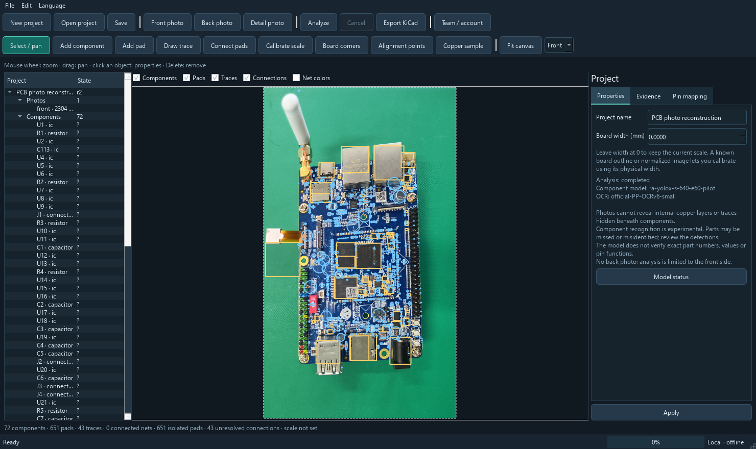
Inspect the photo, component list, and evidence together. Toggle layers, take measurements, and save your corrections with the project.
03 / PILOT LIMITATIONS
Know what is visible.
Keep the unknowns open.
This release assists investigation and editing. A fabrication-ready board still requires human review and electrical measurements.
- Component detection is experimental.
AP50 on a limited photo group: 0.1654. Components may be missed or misclassified. This does not measure electrical connectivity accuracy.
- Hidden copper remains unknown.
Inner layers, connections beneath BGAs, and unmarked component values cannot be verified from the images.
- Proposals require confirmation.
Proposed connections are not automatically added to electrical nets. The KiCad output is a draft using generic symbols and observed geometry.
04 / GET STARTED
Start at
your workbench.
Explore editing and KiCad export with the sample project. When you move to your own board, verify every candidate again.
Your first projectWindows x64
RA PCB 0.1.0 PRIVATE PILOT
General desktop distribution is not available yet. If you already have a pilot copy, the guide explains how to get started.
Demo project · not an accuracy benchmark
05 / COMMON QUESTIONS
Before you begin.
Can I analyze board photos on this website?
This website introduces the app, provides its guide, and includes an illustrative demo. It does not upload board photos or run cloud analysis. Actual image analysis runs in the desktop app.
Is one photo enough?
A single front photo supports limited analysis. Capture both sides under controlled conditions for more visible evidence. Cross-side connections are not verified without reliable alignment.
Are the schematic and PCB ready for fabrication?
The outputs are editable KiCad drafts. Verify component identity, actual pin numbering, pad geometry, and electrical connections against the board. A physical PCB file requires scale calibration.
Do my photos stay on my computer?
For local projects, analysis and saving happen on your computer. If you explicitly choose team sync or optional cloud assistance in the desktop app, the relevant images are sent to the configured server. Read about privacy and product limitations.
What about OpenAI and team features?
The app includes server infrastructure for these integrations. A running service, OIDC sign-in, and the necessary server keys must be configured separately. This website does not create accounts or take payments; subscription integration is limited to Stripe test mode.