
GETTING STARTED / DESKTOP PILOT
From photo to draft.
Six practical steps.
Capture the visible faces of a board, review the suggestions, and carry evidence-supported connections into an editable KiCad project.
This guide is for the desktop application. The website does not upload board photographs or run analysis. The desktop release is a private pilot; no public installer is available on this site. You can download the small demo archive.
If you have the pilot application, open the demo with File → Import archive. Choose an empty project folder. The demo is a drawn board; it does not measure recognition performance on real photographs.
An ordinary photograph cannot reveal inner copper layers or connections hidden beneath components. Unreadable part markings and unmarked values should remain unknown.
Capture both faces clearly.
Place the board on a flat surface. Keep the camera as perpendicular to the board as possible and use soft, even lighting. Scanner images can also be used. Include the complete board, its corners, and reference holes.
- Capture the front and back separately. Keep shared holes and the board outline visible in both photographs.
- Avoid glare, motion blur, and hard shadows. Take additional close-ups of small component markings.
- Create a new local project, then use Front photo, Back photo, and, when needed, Detail photo to add your images.
- Use JPEG, PNG, or single-page TIFF. Record a known board dimension or a reference distance you can measure.
Check perspective and face alignment.
Use Board corners on the original photograph to select the top-left → top-right → bottom-right → bottom-left corners. Follow the same order for the back face. Run analysis to create the rectified view.
If automatic registration is unreliable, use Alignment points to select the same physical locations in the same order on both faces. At least three shared points are required; four holes spread across the board make a better starting point. Select Finish points, then analyze again.
Do not mirror the back image manually; the alignment step accounts for this. Check that shared holes coincide before accepting connections between faces.
Run the local models.
Select Analyze or press F5 to process the photographs, detect component categories, read markings, and extract visible copper geometry. Local analysis requires no account or network connection; the pilot's bundled models run on your computer.
If copper selection is poor, use Copper sample to select a representative copper or trace color, then analyze again. With only one face, the result is limited to that face. Read the analysis warnings when the process finishes.
Detections are candidates. The pilot component model scores 0.1654 AP50 on its limited held-out test group and misses or misclassifies components. This metric does not measure netlist correctness. No electrical net-accuracy benchmark on real boards has been established.
Correct components, pads, and connections.
Choose an object with Select / move and inspect its properties in the right panel. Add missing components or pads and correct the category, position, or dimensions. Use undo and redo to review your changes.
Supported by visible copper continuity. This is not an independent electrical measurement.
A pad connection you have reviewed and confirmed. Check the pin mapping separately.
Excluded from electrical nets. Proposed connections appear as dashed orange lines.
Connect pads adds a user-confirmed connection between two pads. Use it when you have supporting evidence. A newly drawn trace starts as a proposal. Recognizing a component category does not verify its manufacturer part number or actual pinout; leave unseen pin functions unresolved.
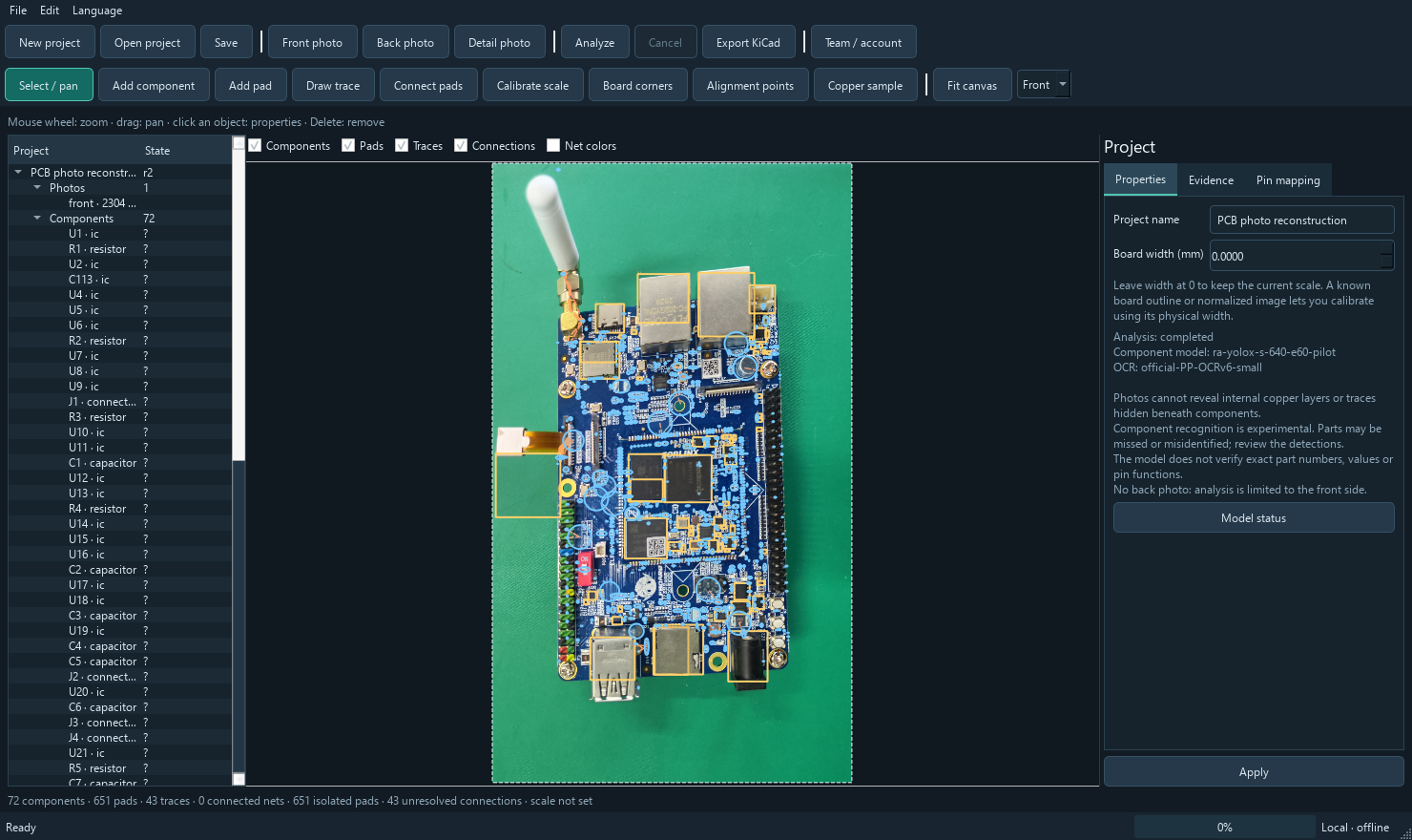
Connect pixels to a real distance.
Select Calibrate scale in the rectified view. Click both ends of a distance whose real length you know, then enter that length in millimeters. For example, use the distance between two mounting holes measured with a ruler.
Do not enter an estimated board width as a measurement. After changing a photograph or its perspective correction, check whether calibration remains valid and measure again if needed. Pad and trace dimensions in the physical PCB draft depend on this scale.
Take an editable draft into KiCad.
Select Export KiCad and choose an output folder. The export includes a schematic, netlist, BOM, and uncertainty reports. With a known scale, it also creates a physical PCB draft and the required local footprint files.
Proposed and unknown connections are excluded from electrical nets. An unknown connection is not marked as an intentional no-connect. Do not confuse generic symbol and pad labels with verified manufacturer pin numbers.
Open the files in KiCad and inspect the schematic and layout. ERC/DRC checks performed through an available KiCad CLI assess file and design consistency; they do not prove electrical equivalence to the photographed board. The output is a draft for review and editing.
WHEN YOU GET STUCK
Three common situations.
I have a schematic, but no physical PCB file.
The application does not create a physical PCB file without a known scale. Calibrate a known distance in millimeters on the rectified image, then export again. A schematic and netlist draft can still be exported without scale.
The result looks outdated after replacing a photograph.
When a source image changes, its geometry and calibration need to be checked again. Select the corners and shared alignment points, then rerun analysis. Review your previous manual corrections against the new photograph; project warnings may flag invalid scale or alignment.
A line appears on screen, but the netlist has no connection.
Check the line's state. Proposed, unknown, and rejected connections do not form nets. Inspect visible continuity and the correct pad-to-pin mapping; confirm the connection when the evidence supports it. Do not accept a proposal simply to complete the netlist.
Pilot test coverage: The Windows desktop workflow has been verified. Linux packages have not been built or run in this work. There is no manually verified PCB-marking OCR evaluation or real-board electrical net benchmark yet.
Read Privacy & limitations to understand where photographs and project data are processed.